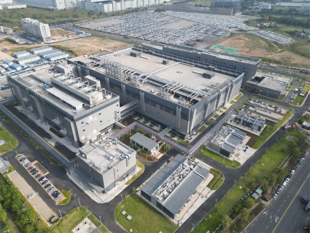
Recently, the Guangzhou Zengxin 12-inch advanced intelligent sensor wafer manufacturing mass production line project undertaken by China Construction Fourth Engineering Bureau successfully passed the completion acceptance.
The project is located in Zengcheng District, Guangzhou City, Guangdong Province, with a total construction area of about 200,000 square meters. The construction content includes production plants, integrated power stations, silane stations, Class A warehouses, hazardous waste warehouses, bulk gas stations, production dispatching buildings, etc.
As the first 12-inch intelligent sensor wafer manufacturing production line project in the country, it will have an annual production capacity of 240,000 12-inch wafers after completion. After commissioning, the products produced are mechanical, acoustic, microfluidic, biological and other sensor devices and supporting ASIC chips, which will gradually form an industrial agglomeration effect, provide high-quality development support for domestic intelligent sensors and related industries, and help the construction of the "Guangdong Strong Core" project.
From production line design to process breakthroughs
The 12-inch wafer production line has significant advantages over the traditional 8-inch production line: the output of single wafer chips is increased by 2.5 times, and the unit cost is reduced by more than 30%. The core breakthrough of the Guangzhou Zengxin Project lies in the adoption of the "Beyond Moore's Law" technology path, which solves the problem of co-design of sensor devices and ASIC (application-specific integrated circuit) chips through three-dimensional integration and heterogeneous material fusion processes. For example, microfluidic sensors need to integrate micron-level fluid channels on the wafer, which places extremely high requirements on the clean room level (Class 100) and temperature and humidity control (±0.1℃ accuracy). The project team has achieved nano-level particle control in the production environment through modular plant design and intelligent control systems.
The supporting silane station, bulk gas station and other facilities reflect the supply chain localization strategy. As a key semiconductor material, silane is adopted in the project. The "on-site gas production + dual-circuit gas supply" mode reduces the risk of raw material transportation by 80%; and the integrated power station integrates ice storage and waste heat recovery systems, which reduces the overall energy consumption by 15% compared with traditional wafer factories.
A 300-acre sensor industrial park has been planned around the project
The strategic value of the Guangzhou Zengxin Project lies not only in the increase in production capacity, but also in its role in integrating the industrial chain. According to statistics, a 12-inch production line can drive upstream material and equipment suppliers and downstream packaging and testing companies to form a 1:5 output value amplification effect. At present, a 300-acre sensor industrial park has been planned around the project, attracting more than 20 upstream and downstream companies such as Hanwei Technology and Goertek Microelectronics to settle in, initially forming a vertical ecology from design, manufacturing to packaging and testing.
Guangdong Province has continued to promote the "Strong Core Project" in recent years, and plans to exceed 400 billion yuan in the scale of the integrated circuit industry by 2025. The commissioning of the chip-enhancing project will complement the existing resources in the Greater Bay Area: Huawei HiSilicon and Pengxin Micro in Shenzhen provide design support, Zhuhai Yueya lays out packaging substrates, and Guangzhou Yuexin focuses on analog chip manufacturing, jointly building a full-chain capability covering "design-manufacturing-application".
The current global sensor market size exceeds US$200 billion, but 80% of the high-end MEMS sensors are monopolized by foreign companies such as Bosch and STMicroelectronics. Taking pressure sensors as an example, the localization rate is less than 15%, and the automotive electronics field is even more dependent on imports. After the mass production of the chip-increasing project, it is expected to meet 40% of the domestic demand for smart sensors, and reduce the cost of key components such as medical CT detectors and TWS headset accelerometers by more than 25%.
More strategically significant is that the project will promote the verification process of domestic equipment. Its production line has introduced domestic equipment such as China Micro Semiconductor Etching Machine and North Huachuang Thin Film Deposition Equipment, and the localization rate of equipment has reached 35%, which is 10 percentage points higher than similar domestic production lines, providing a test scenario for the research and development of process equipment below 14 nanometers.
With the commissioning of the project, China's sensor industry is expected to achieve three major leaps: First, in the field of biosensors, combined with the advantages of Guangzhou's biomedical industry, develop gene sequencing chips for point-of-care testing (POCT); second, relying on the Greater Bay Area artificial intelligence cluster, develop intelligent sensing systems integrating AI algorithms; third, explore cutting-edge directions such as quantum sensors to provide next-generation perception solutions for 6G communications and autonomous driving.
This paper is from Ulink Media, Shenzhen, China, the organizer of IOTE EXPO (IoT Expo in China)


